 |
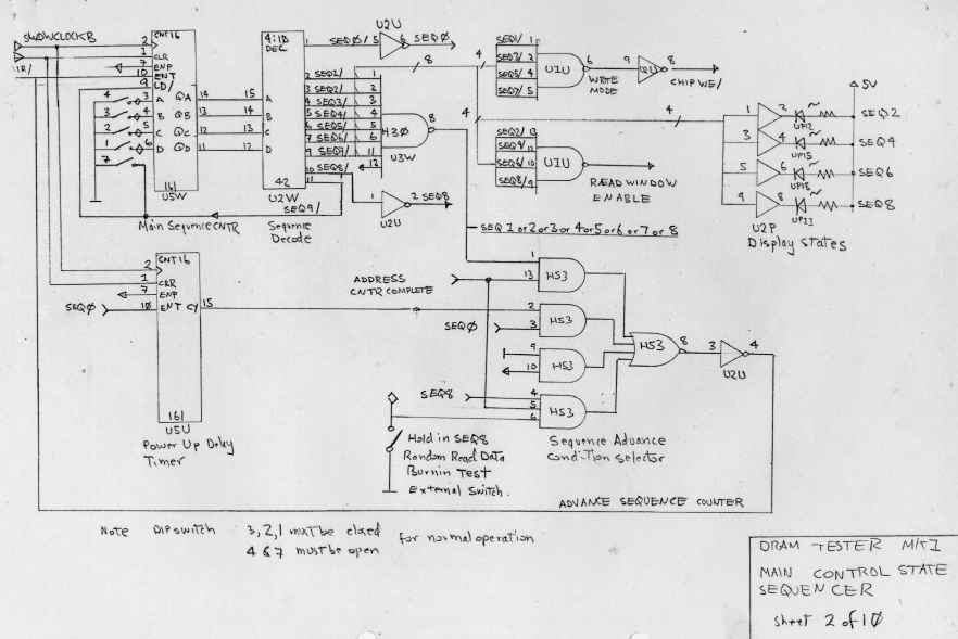 |
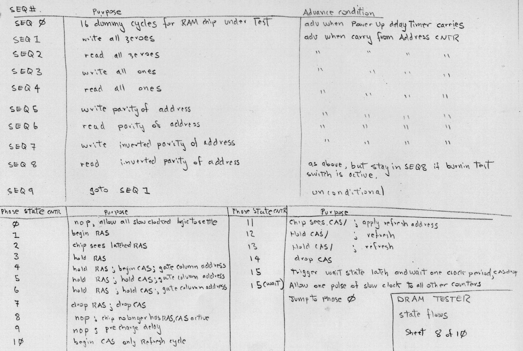
The main sequencing, read write control, done with this microsequencer.
Tests included a burn in test, data once written could be read forever
untill error was detected and flagged. This machine was microprogrammed by a simple map of concept/intention to wire.
|
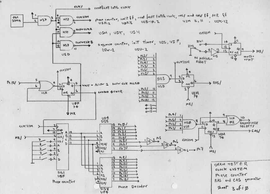 |
microsequencer for generating chip RAS and CAS and clock
distribution. The raw RAS and CAS signals from the phase decoders are
cleaned up by D flip-flops to eliminate glitches. Note the use of
multiple input gates used to create arbitary digital waveforms by
decoding the complete count and then just ANDing all the required unary
bits. This permits the simple generation of arbitary waveforms.
RAS/CAS generation is just one such application. Never attempt to drive
RAM control signals through decoded logic unless the edges are
qualified by a D flip flop. You simply cannot design away the decoding
glitches and clean edges are very important to RAM.
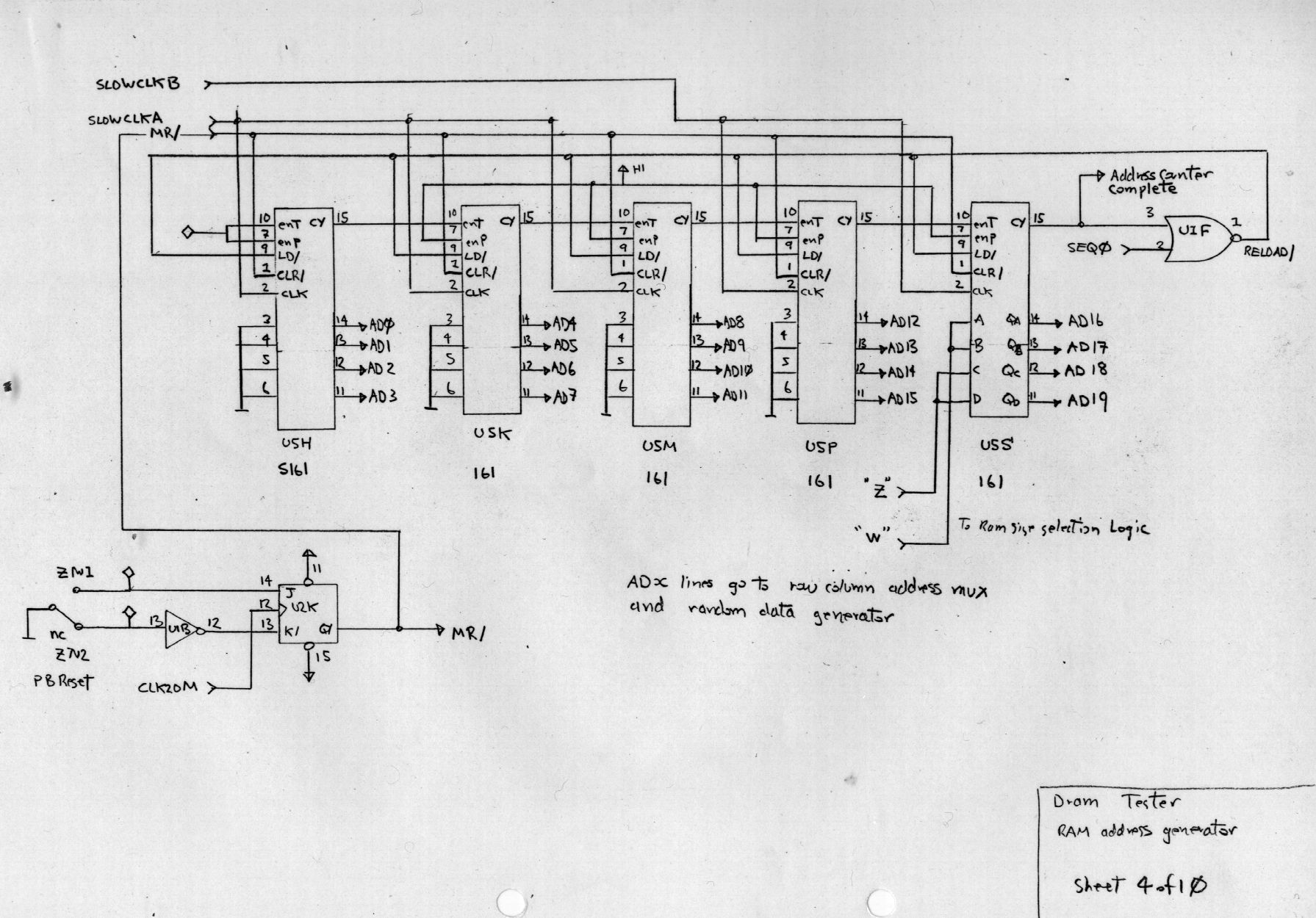
The
slowed clock was supplied to the chain of 4 bit counters that generated
the ram address. At 20Mhz, these four bit counters were too slow
to permit continuous clocking, so this is a semi-synchronous logic.
Four cascaded counters could generate and propagate a clean CARRY
OUT signal, but five of them would produce an unuseable carry signal.
This is because , sadly forthese chips, the CARRY signal had to
propagate through too many internal gates in series. So, how then to
generate a reliable 20 bit counter at 20Mhz ? The clock pulse
could still be 50ns but here we issue one clock pulse to the
counter clocks and wait for the CARRY signal to settle. Here we
stall the main machine clock , once for each unique address to be
generated, while we wait another 100ns to be sure that the counters
have settled into a "believe-able" state. We would not have had this
problem if this had been done with ECL !
|
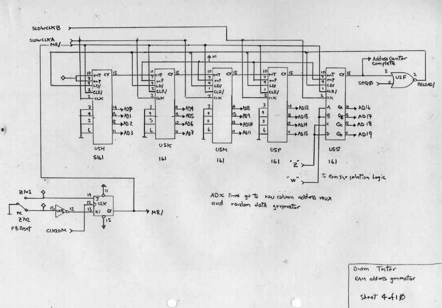 |
| Logical address bits generator,
nothing more than a 20 bit
counter. Because of the long carry propagation delay this counter
needed a gated clock rather than run synchronously. Gated clocks break
the simple synchronous paradigm but are a requirement when long
multi-gate and multi-package have a long serial delay path as the
counter carry signal requires. I tried to use look ahead carry but the
design effort was beyond me. The master-reset signal is created by cleaning up the reset switch with a JK FF. |
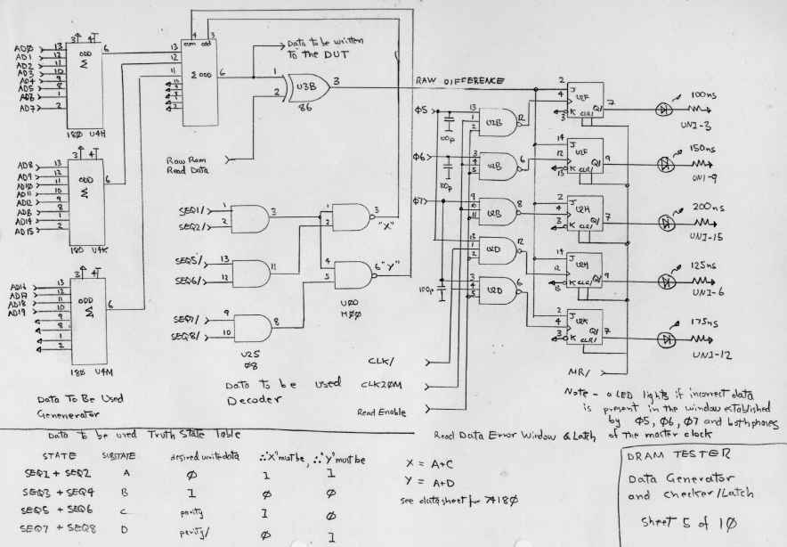 |
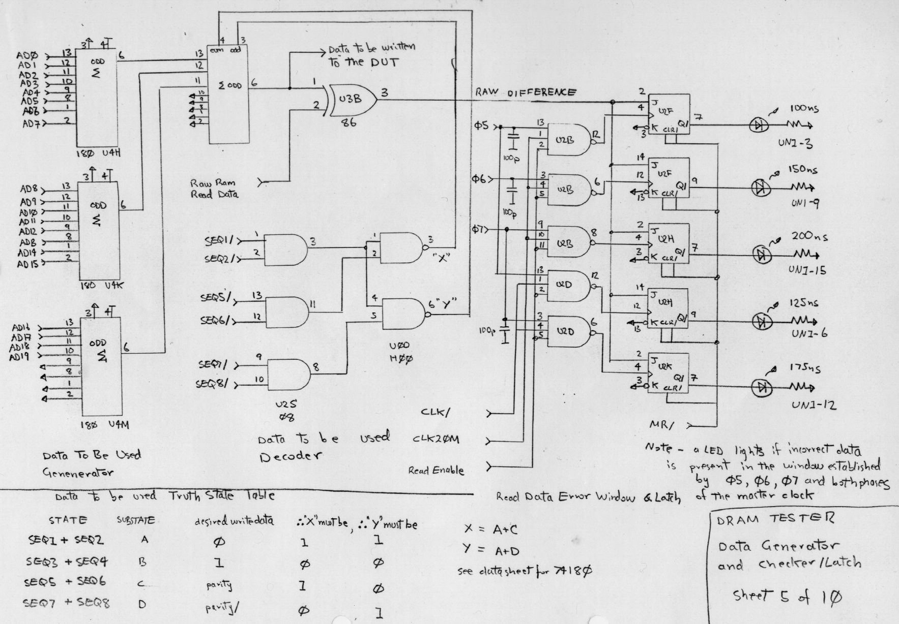
data
for one bit wide drams was
generated by getting the odd and even
parity of the address bits and writing that. This gave a reasonably
thorough test of the drams ability to decode its address bus.
This tester could measure access time by gating read back data at
differant sample times. It revealled that 200ns drams could be run at
100ns if you kept them cold! read back data is compared in the XOR
gate. The JK flip flops are clocked on various delayed clock edges and
record that state of the data comparison. The SEQ counters are decoded
and drive the 74180 parity generators. They had control inputs to make
the 74180 generate a selection of odd parity, even parity, ONE or ZERO.
The raw readback data from the DRAM was compared with the
exclusive OR gate and the data which had been written. Its state was
latched in the JK flip flops whose individual clocks were derived from
assorted delayed edges of the main system master clock. The
effect was to measure the time at which the data read back became valid.
|
 |
 |
|
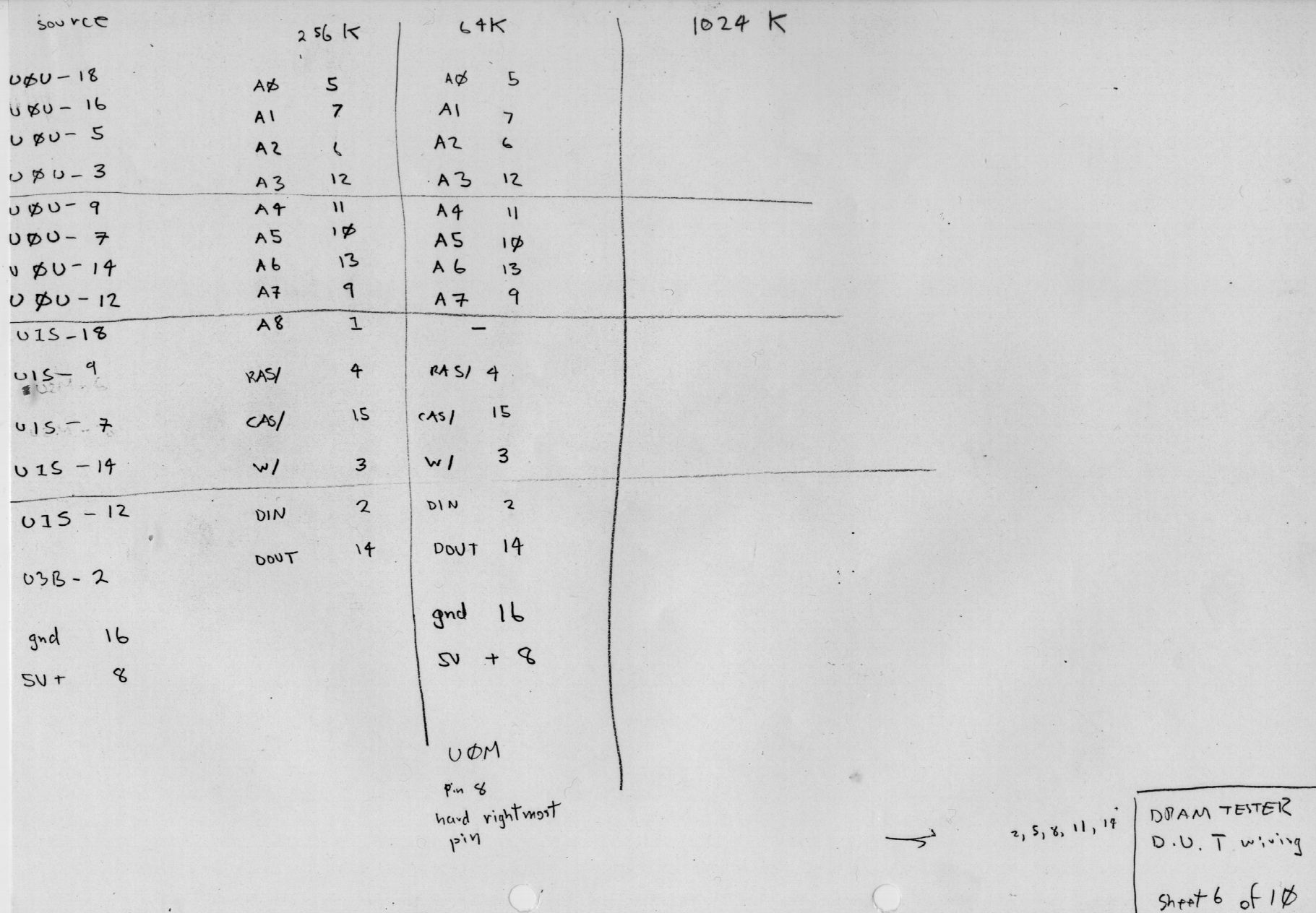
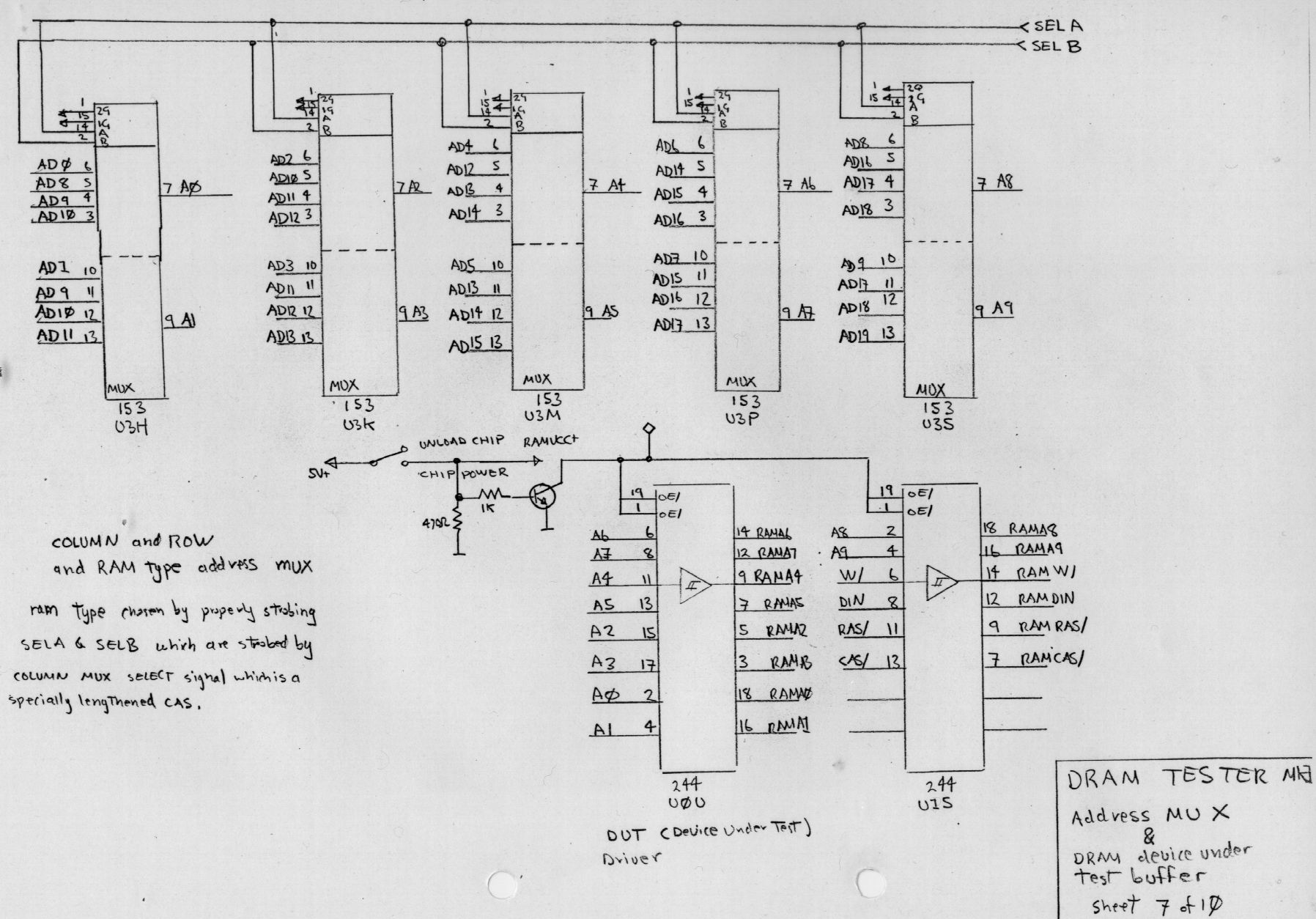
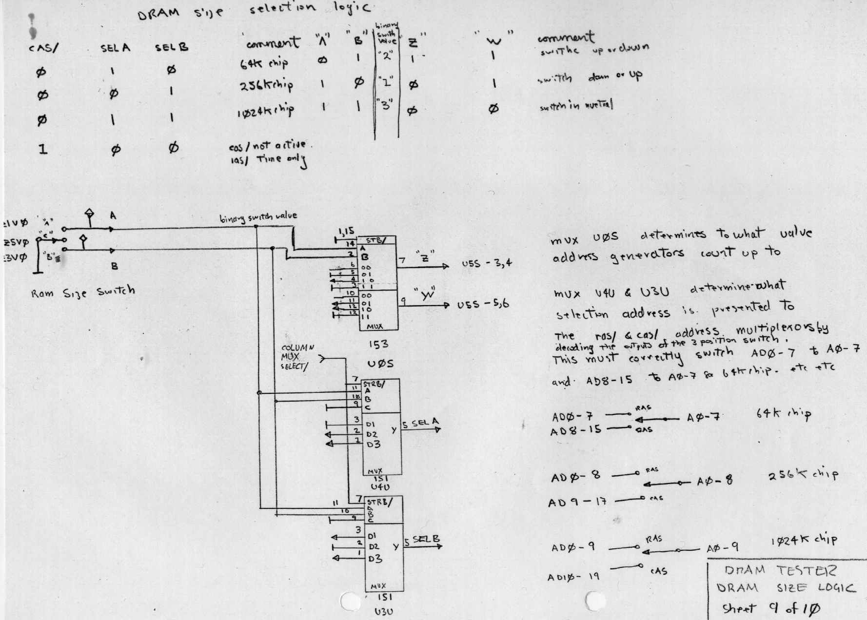
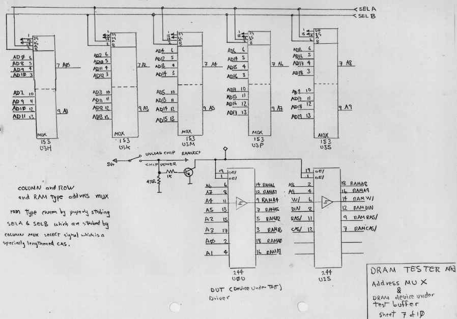
logical ram addresses are mapped to physical chip addresses pins as a
function of the chip type by this MUX array. A switch permitted the
device-under-test to be reloaded while the machine was powered up by
tristating the drivers |
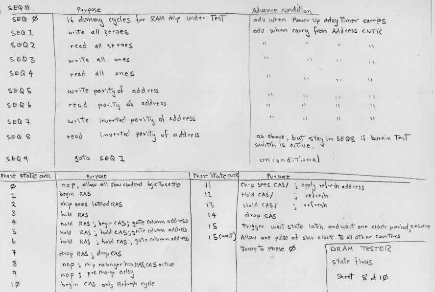 |
| This is the "plain language"
microprogram for both
microsequencers. This allmost directly maps to the wiring of the
machines. There are two micro programs here. There is the phase
sequencer that is responsible for creating the RAS and CAS dram signals
and controlling the dram address mux and ensuring the setup and hold
time requirement of the dram is satisfied. The main sequence
generator contains the high level program that orchestrates the
complete test program. Its a direct application of the zero-bit-computer paradigm |
 |
|
logic that selects the right address lines to chip address lines for
differant sized ram chips. Muxes are used to generate arbitary logic
functions, rather than random logic. Errors in design or logic analysis
are easily rectified by reallocating ones and zeroes to the mux inputs
rather than completely redesigning a random logic wiring map. |
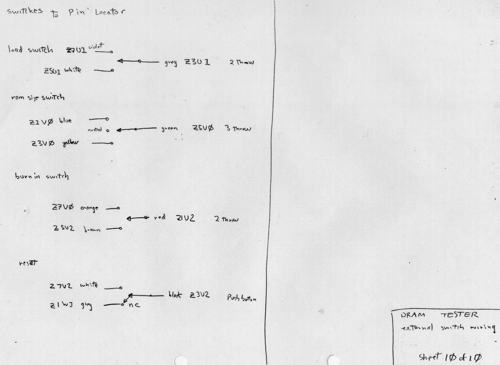 |
| assigning external human switches to their meanings and wiring on teh board |
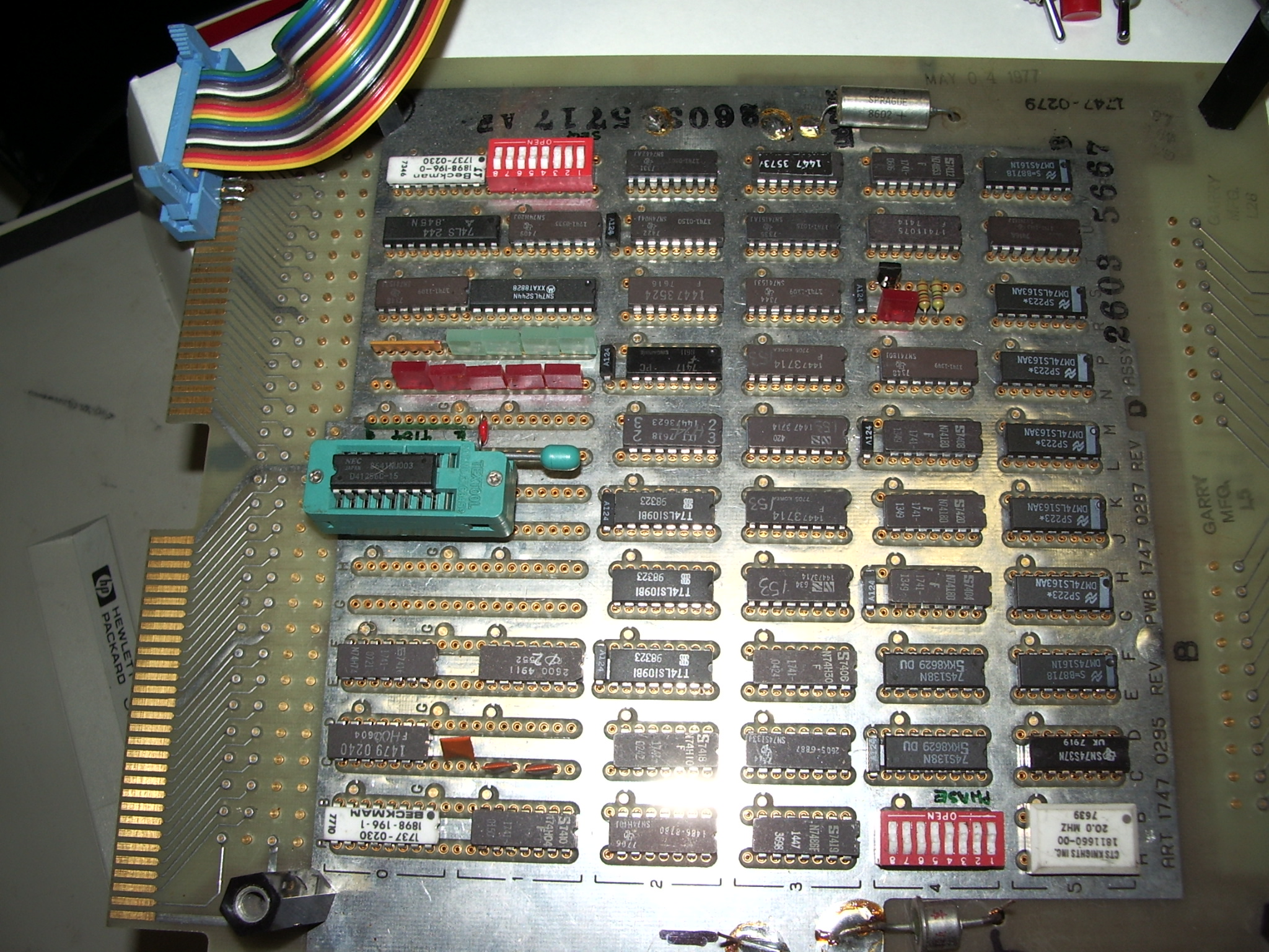
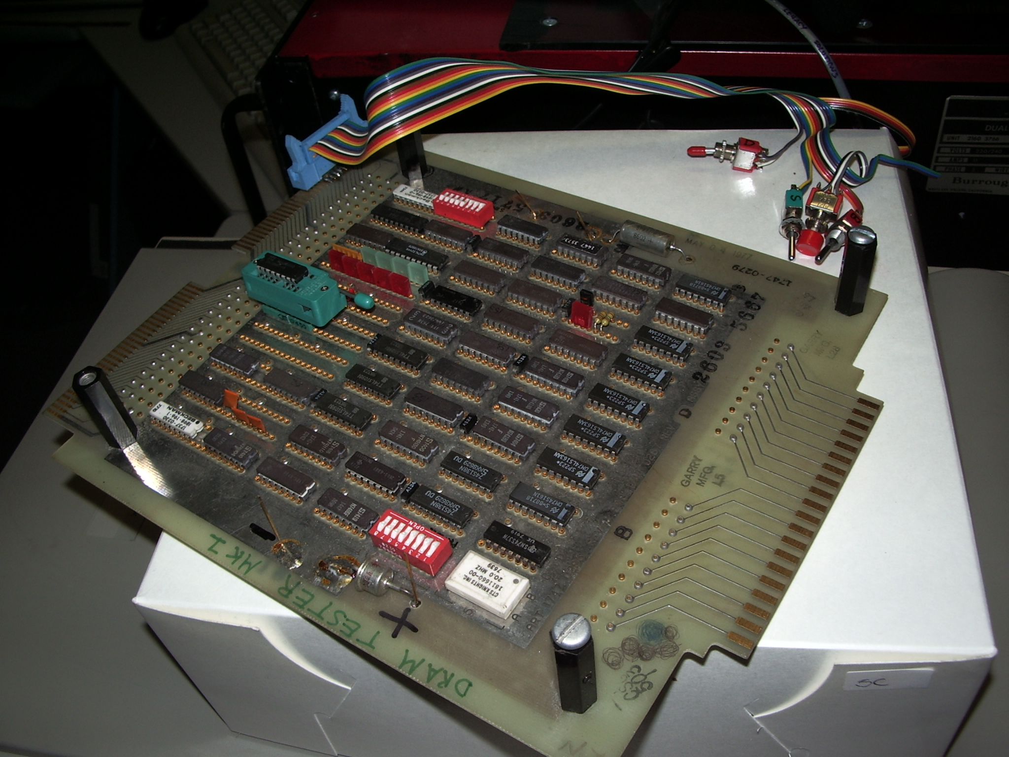
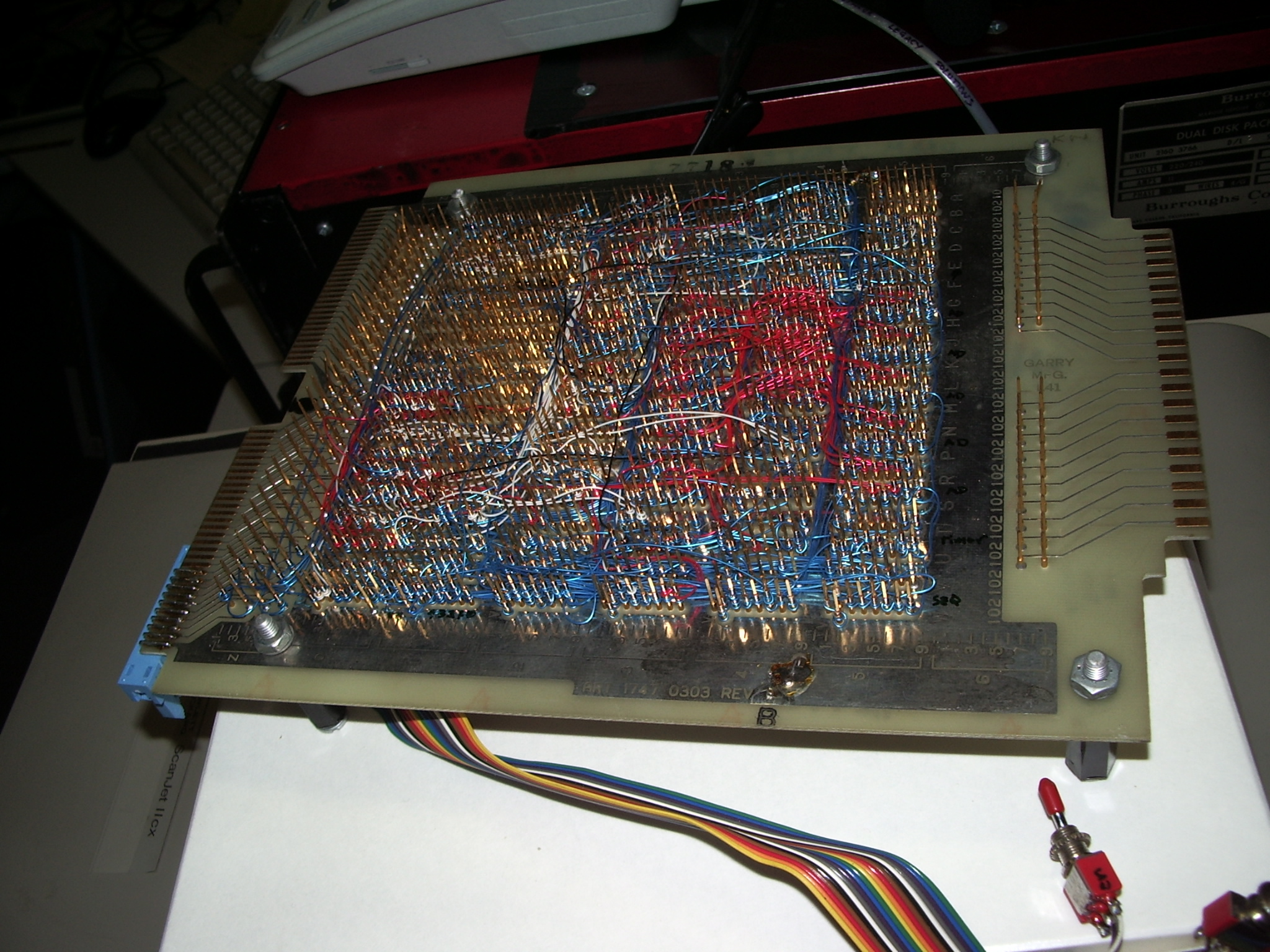
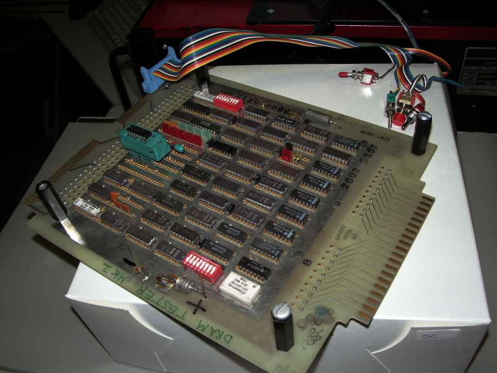
| The Project as built. The wirewrap cards came from an Burroughs mainframe that I used to maintain, a long time ago |
 |
 |
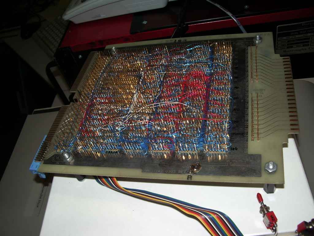 |
| wirewrap is really to only cost effective method for one off projects like this. |