The Zero Bit Computer
a simple micro sequencer or algorithmic state machine design
by Ralph Klimek June 2007 based on work by author from 1987
abstract: simple concept, MSI implementation of a micro sequencer
permits one to one mapping of natural language sequence description to
direct implementation in MSI logic without the ledgerdermain of state
machine design and logic minimization.
This simple design was first brought to my attention in Blakeslee (1)
as a simple way of implementing algorithmic state machines. Traditional
state machine design involves a rigid state description, input
contingencies , output state to next input state mapping, followed by
assignment of discrete states to JK flip flops and then logic
minimization with Karnough maps or other such tools that in my opinion
serves only to obfuscate the problem and deny practical implementation.
Any change whatsoever in the requirements in the machine neccesarily
require its complete redesign and rebuilding. The traditional method
admits no possibility of "programming" to cope with design changes. In
practice, the traditional state machine permits no simple debugging,
sequence single stepping to verify design compliance. The final logic
map does not have an intuitive mapping between the logic and the
function that the machine has been designed to perform.
The key elements in the design are 4 bit binary resettable counters
with clock enable and preset enable inputs, binary to unary decoders
(eg 74154 4 to 16 decoder) , 8 to 1 multiplexer (eg 74151), 4 bit
priority encoder (eg 74148) and simple SSI glue logic.
Applications.
This design technique is applicable only to seventies era logic when
MSI gates became available and situations where the raw speed
adavantage of hard wired logic or the simplicity of the problem does
not require the complexity or expense of developing a microprocessor
based solution. In this day one would be remiss not to use an AVR or PIC for even the
most trivial applications unless speed is important. The simple
74xxx series logic can run at at least 20Mhz, newer ACT or older S
variant logic may toggle up to nearly 100 Mhz. The design
implemented in ECL can easily run at 200Mhz without special design
effort.
The design presented and implented in typical 74 series logic will have
a maximum of 16 states. In the practical applications presented (
Static and Dynamic RAM chip testers ) the machine will have millions of
states.
The most usefull and critical application of the the zero bit computer
is in the generation of precision and deterministic timing
sequences for such things as dynamic ram signal sequencing, CCD array
timing, microprocessor bus control or even control of simple automata.
The natural language problem description should be able to be stated in terms of these constructs.
1. wait until condition, or advance state until condition, or advance state unconditionally
2. branch to state X on external contingency, branch to state X if
state equals Y (being an internal contingency), unconditional branch.
3. for each state, there exists a discrete unary output signal, used or
unused, whose meaning is arbitrary and defines the usefull output of
the machine.
These statements map directly to a logic map consisting of nothing more
than a counter, decoder, and two multiplexors and a priority encoder
(only if more than one branch destination is required).
There is no logic minimization, there is nothing to minimise in this MSI implementation. ( still worth doing in an FPGA)
This simple design cannot do arithmetic or branch on value comparisons
and cannot operate on DATA, hence the origin of the zero bit computer
idea. It is not a micro processor, however some conceputally simple
extentions could turn it into an arbitarilly powerfull RISC processor.
An 4 bit MSI counter generally has a clock input, clock enable input, a
preset state input control, preset inputs and binary state outputs.
Some may have a count direction control but that is not a usefull
function in this case. The preset enable control signal should be
synchronous.
A priority encoder take unary signals and outputs a binary word. A
multiplexer takes a binary address value and selects one of many input
unary signals and passes it through. A decoder takes a binary value and
generates a unary signal that represents the binary value. The state of
the machine is defined by the weighted binary value of a small number
of D type flip flops, which in our case are embedded in the binary
counter chips which with their internal glue logic compel them to
"count" in binary. Counting in this sense is just a unique but
arbitrary mapping of one state to its next state however as human
designers we allready understand the "counting sequence"
0,1,2,3.....14,15,0 so there is at least one less mystery to deal with.
The "clock" signal may be any free running clock , the clock serves
merely as a source of discrete time steps that define the smallest
atomic state transistion time and more importantly provide positive
edge transistions that D flip flops require in order to change state.
Now is the time to connect some of these logic gates together.
The preset enable of the counter is connected to the ouput of a
multiplexer. The address line inputs of the multiplexer are connected
to the counter outputs. The data inputs to the multiplexer
are connected to logical zero or one or an external input fromthe
outside world. When the preset input of the counter is active the
binary value present on the counter data input lines becomes (and this
is the important bit) BECOMES THE NEW STATE. This setup can now
perform conditional and unconditional branching determined only by THE
INPUTS OF THE MULTIPLEXOR. Nops or "just advance to the next state" are
wired as logical zeros, unconditional branches are wired as logical
ones and conditional branches are wired to the outside world.
Allready this little machine can react to external stimulie in a meaningful way.
Each state of the machine must have assigned to it a "meaning" in the
higher language sense. The state is represented by the weighted binary
value of the counter. The counter outputs now also feed a binary to
unary decoder. Now exists a discrete signal to which we attach
meanings, even if a particular state is not used, redundant or
"meaningless" we still assign a meaning of "not used" to it.
These unary outputs also represent the "usefull" output signals that
might be driving bus control signals, LSI control signals,
relays, lights, whatever. It is possible to connect one of these unary
outputs to the preset enable multiplexor input to implement a "when you
have reached the end of the program branch to the beginning "
construct...or also to catch and manage unimplemented states ( which
all good digital designers take care of ... dont they ?)
To implement the wait on condition function or the advance state
control another multiplexer output connects to the clock enable
signal of the counter. The address lines to the multiplexor and
counter ouput are connected. It is now possible to assign a wait
states based on the state of the counters. Logical ones
will advance the state, logical zero will halt the machine (this is not
so useless...we may wish to halt on some alarm condition ) or an
external signal. The state machine can now be programmed to wait UNTIL
some external condition is satisfied.
Now we can add more advanced features. The data presented to the preset
inputs of the counter represents a program address location in the
sense of the way we understand what programming means.
Typically it would be hard wired to all logical zero as most micro
programms will branch unconditionally back to zero. We might however
branch back to 0001 and leave state 0000 to perform power on
initiallization of other systems. We could feed the preset inputs
through another multiplexor to implement a conditional branch on
external condition. If there are many external signals on which we wish
to conditinally branch , feed them all through a priority encoder
which will generate a binary weighted word mapped to any one of its
unary input signals. (Think of a priority encoder as a kind of PROM
whoose contents is selected by unary coded address lines!)
There are some logical extentions to this simple scheme to make it more
complicated. Sixtenn states may not seem much and isnt enough for all
but the most simple control and sequencing requirements. Multiple
counters can be cascaded but even with a state counter of 8 bits, this
gives 256 states. Decoding all these states is unreasonable with
discrete logic, only the actual uniquely required states would be
decoded, an application might be TV sync generation where we require 16
bit time resolution. More complex control would be implemented in a
ROM. The counter outputs address a ROM some of whose outputs are
connected to the "branch enable" and "clock enable" and by now the ROM
contents look suprisingly similar to assembly language.
This system is still not processing data, in this model processing data
means makeing conditional branches based on the outcome of arithmetic
operations. Now a "data" path needs to be defined. This can as
arbitarily complex or simple as required. Sources and sinks of data
must be defined. A source of data could be external binary words,
binary words from some ROM output lines, binary words from RAM,
binary words from a general purpose register and so on. Then logical or
arithmetic operations need to be defined. There exists chips allready
prewired to perform arbitrary operations on two binary words that are
selected by some address lines (for example the 74181 ALU slice ) In
our case those selection lines are driven by some of our ROM output
signals. Other ROM or RAMoutput signals could be a source of this data
too. The ALU has two input streams, one output operation
result stream and CONDITION CODES that typically indicated whether
arithmetic operations were meaningfull, overflow, underflow , zero ,
arithmetic carry flag, shift carry. These condition codes may be
directly connected to the branch enable multiplexor. Now programmatic
control based on arithmetic/logic operations becomes possible. With
many branch destinations it make sense that they are supplied by the
now big ROM as well.
The ALU has not only condition code outputs but a data output. This
"processed data" needs a home. This could be routed via more muxes to
the input of RAM, a display, a register or whatever. The RAM write
enable signal is supplied by a one bit output of the ROM , now our
program repertoire includes a WRITE to memory operation.
It is not difficult to perceive that here is the making of a simple completely general purpose computer of arbitrary word size.
Presented here are two zero bit computer based machines I have
constructed to perform an actual needed task that at the time could not
be easily done with a microprocessor. The design is twenty years old
using thirty year old components to solve a problem twenty years ago!
a simple and effective static ram testing machine based on ZBCs
a machine for testing dynamic ram based on the Zero Bit microsequencer
Reference 1 Digital Design iwth Standard MSI and LSI, Design
Techniques for the microcomputer age 2nd edition by Thomas
R.Blakeslee (Wiley) 1979
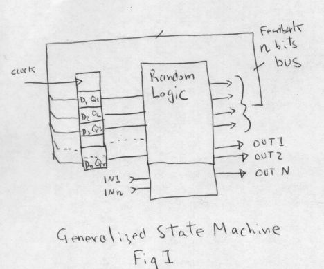 |  |
| The generalised state machine | understanding the operation of the D flip flop |
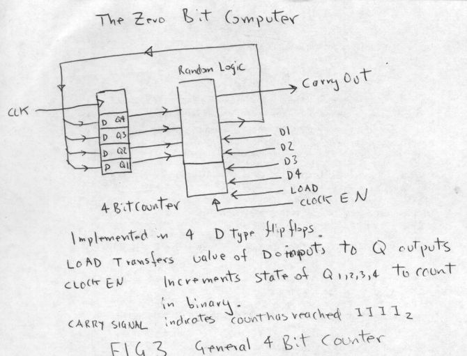 | |
| The zero bit computer (with 16 possible states/steps) | |
The zero bit microsequencer concept should also be understood in a
newer way of understanding the operation of combinatorial logic.
The classical view is that of the philosophical logician that
models behaviour in terms of truth tables . This view is correct,
and is the ultimate source of wisdom when the particular behaviour of a
logic map needs to be uniquely specified. It is, however,
difficult to turn the truth table into a humanely understandable or
meaning form. The logic elements should be understood in terms of
signal flow. Real digital devices deal with dynamic situations and real
physical conditions. They have an effect on to the signals presented to
them. They should be thought of as small control elements that are
presented with a generalized concept of signal, a signal flow and a
control element and maybe a transforming element. It is not usually helpfull to view them as logic because real brains do not generally think logically.
 |  |
 |  |
 | just
some notes I was writing before committing myself to actually
doing this article. Click on them to view the full resolution. |
Ralph's Elements of Digital Logic
warning. The author is neither a qualified academic or engineer so he is excused from the burden of orthodoxy !
Binary and Unary signals.
A unary signal is one that has meaning only when asserted. When it is not asserted it is meaningless.
It is not correct to say the logical inversion of a unary signal means the opposite of the meaning!
A Binary signal is such a signal whoose meaning is "invertable"
A binary weighted signal is a group of signals whoose place position has meaning.
The logical inverter or NOT gate.
Not the simplest digital logic element! Not by any means. It merely
flips the polarity of a unary signal or inverts the meaning of a truly
binary signal. You will discover that very few digital signals
are "binary" in meaning ( at least by my definition) Inverters
are very necessary glue logic because signals emitted by MSI logic is
often the wrong polarity for immediate use.
The AND gate.
Put the truth table aside for now. The AND gate is the simplest
to understand as the first gate that has a control line. A two
input and gate passes a signal without tranformation if the control
line is logically HI. (or true, or greater than 2.4 volts or whatever
you define it to be!)
A multiple input AND gate is the simple concatination of two input AND
gates. It has the property of being a detector of ALL ONES,
or detecting if AT LEAST one input is LOW.
The AND gate is the most fundamental biulding block. Now you may look at its truth table.
The OR gate.
Put the truth table aside for now. The OR gate is just an AND
gate in disguise. The logical operations of ORing and ANDing are
complementary. This isnt news, every good digital design book
belabours this point. A signal presented at one input will
flow unimpeded if the CONTROL line is logically LO. Just add
inverters as glue logic to correct the signal polarities. NOW you may
look at your truth table.
A multiple input OR gate can detect if any one of its inputs goes HI.
Very usefull for monitoring alarms! (or generating sums of
minterms when you need a complex logic function, hello there
logicians! but dont this...real engineers use a MUX!)
The XOR gate.
Put the truth table aside for now. This is a two input control
element and is the first simple element that can transform data. The
XOR gate is an equality detector (check the truth table) and it
is a programmable inverter. It inverts the signal if the control
line is LO, or just hands the signal along if control is HI. Very
usefull for programmatlicaly flipping meaning in a binary signal, very
usefull for detecting when things ARE the SAME ! Multiple input XOR gates perform the parity checking/generation function.
The MUX or multiplexor.
The simplistic model of a MUX is presented as a programmable signal
selector. It take multiple signal inputs and a binary weighted set of
control signals and passes the selected signal unmolested. It does not
transform the signal. Immediate applications of this
device come to mind, it implements a SELECTION function. Buts thats
only one of its two purposes. It is also a poor man's ROM. One
mux can be used to replace a wharehouse full of random combinatorial
logic to create arbitarily complex logic functions. A MUX is a
programmable logical function generator. It is programmed by
wiring its data inputs to HIs and LOs as required. The signal
inputs now go to what we thought were selection lines! A 3 of 8
mux can generate any function of 3 binary variables. We also use
the mux in the zero bit microsequencer to scan for condition codes.
The power of the MUX for constructing random combinatorial logic arises
during the design phase. If we make a design error ( as we do ) we
merely reassign the pattern of LOs and HIs to to the mux inputs. If we
had used discrete gates we tear up the design (and the hardware) and
start again. There is no performance penalty either.
Example MSI muxes are 74151 and 74154
The n to 2^n DECODER
The DECODER turns a binary weighted parallel signal into a UNARY
signal. Thats all it does. This is probably the most important digital
element. It is only through a vast tree of decoders that any unique bit
in the RAM in this computer and all computers can be reached. The
decoder says "of all the things I can see on my inputs....I found THIS
one...right here..see my unary output signal... and Cower, mere
mortal!"
The cross coupled unclocked flip flop
This is a composite element made be cross connecting a pair of nand
gates or nor gates. Use with care. The only application that there is
for
this awful device is to bebounce mechanical switch contacts. For this
application they are marvellous. Maybe you could use one for latching
an alarm condition , but totherwise avoid it like the plague. All your
flip flops should be clocked and only clocked by using an edge
sensitive D flip flop.
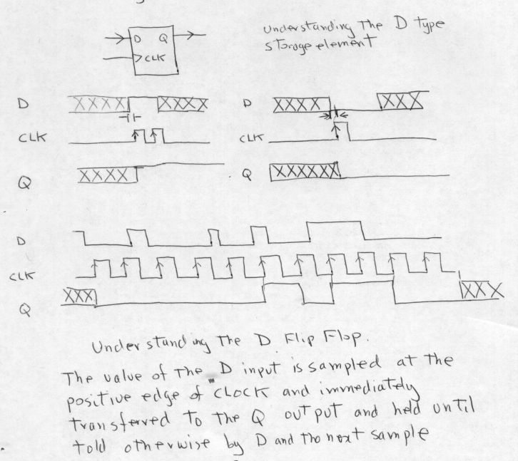
The edge clocked D flip flop.
This is the
only kind of flip flop that is to be tolerated in MSI digital design.
JK flip flops all contain truth table gotchas and other logical
hazards, that never would have thought about will plague your state
machine once it starts running near its maximum speed. A D
flip flop is a one bit memory element, but from a signal flow
perspective , consider it to be a "signal qualification system". This
needs more explanation. Consider what happens when an n-bit
binary word is presented to a tree of logic that has one logical
output. The n-bit binary word may have been presented with all the bit
time transistions occuring at the same instant, but the output of the
combinatorial logic tree will flutter up and down untill such time that
all the un equal propagation delays through the combinatorial tree have
expired. Even though there is but one input word, the output bit value
will/may have transistioned as many times as there are logical elements
in the tree. It means the logical output of ANY combinatorial tree
CANNOT be used for any CLOCKING purpose....because you thought you were
getting ONE state transistion, but in reality you get MANY.
Classical texts call them races or decoding spikes. By feeding
the ouput of any arbitarily complex combinatorial logical tree (eg
decoder, ROM/RAM array etc) into the D input of a type D flip flop and
then clocking it, after an appropriate time delay, (after all the
propagation delays of the tree have settled ) the Q output contains a
beautiful output level that is absolutely stable, and even better, only
ONE output transistion will occur per clock pulse. That means the Q
output can be used by things to whom the absolute quantity of pulses
matters....for example RAM write enable pulses, counter clock inputs. All
signals that are to be used as clocks, such that the number of
transistions is critical, such signals MUST be "cleaned" up with a D
type flip flop. That is what I mean by calling this device a
"signal qualification system". And it is a system, the edge
triggered device has a very complex internal circuit and even
superficially, does not even look like a cross coupled flip flop. The
state of the D input at the very instant of the clock transistion (neg
or positve edge depending on type ) is tranfered and HELD on the Q
output untill such time there is a state differance on the D input at
the time of a clock transistion. It is a kind of filter. It means
that the D input can be noisy, unstable, contain transient
combinatorial spikes, all that does not matter, only the state of the D
input at the instant of the clock edge. Do note put too much note in
the description of the D flip flop in classical electrical engineering
texts. It is described as a "delay element" (hence "D" ) which is
technically correct, off course, but it does not help you in
understanding why the edge triggered D flip flop is so incredibly
important or what it actually does.
the binary counter.
When
Medium Scale Integration TTL circuits were first created, the first
function was the D flip flop, this closely followed by the 4 bit
counter. This device, depending on the model, will present
on its Q outputs all possible 4 bit values, incrementing or
decrementing for every clock pulse, emitting a narrow wobbly pulse on
its carry/borrow output every time the count passes 1111 or 0000. It
may have optional inputs that performs a counter enable signal, or a
reset, or more usefully a present, whereby an arbitary bit pattern may
be set on its D inputs which are immeditely transfered to the Q outputs
on the next clock transistion. The simplest use for a counter
might be to divide the frequency of the clock by some small integer to
get a more usefull clock frequency. The Q outputs of the
counters internal D flip flops are the Q outputs of the counter, and
that means these signal may be used directly as clocks and deteministic
clock edges.
The binary counter finds its application where ever
a controlled repeating binary sequence is required, as in for example,
a counter! , address generator for a PROM, a counter feeding random
combinatorial logic for genearting arbitarily complex pulse sequences,
and as we shall see, forming the primary control element in the ZERO
BIT COMPUTER core.
the Tristate Buffer
Now this is a way of creating and selecting arbitary bit patterns and putting many of them on the same bit of wire. Its
just another mux, really. The only care that is needed is to be
sure never to assert a Tristate bus by more than one buffer at a time.
The resulting Vcc sags will trigger TTL flip flops in a distressing and
random way. It also mangles your precious data ! Just drive them
from from the same decoder, dont trust your microcode to do the right
thing...ALL the time.
the ROM.
Think
of it as an exceedingly complex decoder, converting an abitary input
binary word into an arbitary output word. Funnily enough, this
could also be usefull for program storage ! (this is not news!)
Any computable function or any computer at all can be generated
or emulated by a sufficiently large ROM placed in a feedback loop
between the D input and Qoutput of a suffiencietly large single
register made from D type flip flops. Only a generalised Turing
machine is more abstracted ( or capable) It would be hard work to
write the microprogram to do anything usefull.. that is why real
computers have instruction sequencers and an alu . (I think the
real reason is that ROM is expensive !)
the RAM.
Think
of RAM as being nothing more than gazillions of "D flip flop
registers". (only if properly buffered) Must be usefull for something!
to be continued

Wed May 27 18:58:32 EST 2009; Fri Jul 9 18:33:21 EST 2010
(one day I will finish this article by getting around to the point that I am trying to make.....its harder than I thought!)
home